LPDDR5 and ECC.

Jimmyjames

Site Champ
Posts
675
Reaction score
763
Not sure if this has been discussed, but I thought I’d mention it anyway. On this weeks ATP podcast, the hosts discussed some feedback they received regarding ECC in Apple Silicon Macs. According the feedback, LPDDR5 actually includes ECC in two forms: Array Memory ECC, and Link ECC.

The former is for correcting errors while the data is still on the chip, the latter for then the data leaves the chip and travels to it’s destination.

The M1 had LPDDR4X and all other Apple Silicon Macs have LPDDR5. It seems that both kinds have ECC always on and always working. LPDDR5 also has the option of Link ECC, which can be enabled or disabled in real time! We apparently have no way of knowing if Link ECC is enabled on Apple Silicon or not. Both of these ECC variants provide similar protection to traditional ECC found on the Mac Pro.

I had always thought ECC was a notable miss on Apple Silicon chips. It seems I was just ignorant! Still it’s weird that Apple wouldn’t have mentioned this at all.

Has anyone else heard of this?

The episode is here if anyone wants to have a listen: https://atp.fm/563 starting at 32:15
Also found this: https://semiengineering.com/what-de...ut-error-correction-code-ecc-in-ddr-memories/
 
Last edited:

leman

Site Champ
Posts
641
Reaction score
1,196
Apple has a series of patents regarding LPDDR ECC, but I’d too expect them to mention the feature explicitly, since it has a lot of psychological value. It is very strange if they do offer ECC but don’t talk about it - it’s a widely requested feature.
 

Jimmyjames

Site Champ
Posts
675
Reaction score
763
Apple has a series of patents regarding LPDDR ECC, but I’d too expect them to mention the feature explicitly, since it has a lot of psychological value. It is very strange if they do offer ECC but don’t talk about it - it’s a widely requested feature.
Yes, it is a strange situation. I would definitely expect Apple to have mentioned it, and yet there does seem to be evidence that LPDDR5 does include ECC.
 

Cmaier

Site Master
Staff Member
Site Donor
Posts
5,329
Reaction score
8,520
Yes, it is a strange situation. I would definitely expect Apple to have mentioned it, and yet there does seem to be evidence that LPDDR5 does include ECC.

I think when people are complaining, they are complaining about link ECC? (Or they don’t understand the difference between them).

I’ve always felt link ECC was a dumb solution - just differential signal and you’re immune to injected noise. Twice the wires, but you also buy yourself immunity to a bunch of side channel attacks. Nobody listens to me.
 

Jimmyjames

Site Champ
Posts
675
Reaction score
763
I think when people are complaining, they are complaining about link ECC? (Or they don’t understand the difference between them).

I’ve always felt link ECC was a dumb solution - just differential signal and you’re immune to injected noise. Twice the wires, but you also buy yourself immunity to a bunch of side channel attacks. Nobody listens to me.
Interesting insight thanks.

One thing that was mentioned on the podcast, which I’d be interested to get your opinion on, is whether the very short distance between the ram and the cpu on Apple’s SoC would remove the need for Link ECC. Does distance play a part in how likely errors are?
 

Cmaier

Site Master
Staff Member
Site Donor
Posts
5,329
Reaction score
8,520
Interesting insight thanks.

One thing that was mentioned on the podcast, which I’d be interested to get your opinion on, is whether the very short distance between the ram and the cpu on Apple’s SoC would remove the need for Link ECC. Does distance play a part in how likely errors are?

Well, yeah, short distances help. When you are talking about link ECC you aren’t worried about alpha particles or anything, but are worried about noise being injected by surrounding circuitry. Shorter wires are less likely to have noise injected - wires act like antennae, and shorter antennae are worse at receiving signals. Typically the wires are shielded, swizzled, and/or differential so that they are relatively immune to injected noise in most scenarios. You can also increase drive strength of the drivers so that the signal ramps are short. Where you get into problems are where the wires are long, heavily loaded, or underdriven. That gives ample opportunity for injected noise to be misinterpreted as the wrong signal level.
 

mr_roboto

Site Champ
Posts
288
Reaction score
464
Not sure if this has been discussed, but I thought I’d mention it anyway. On this weeks ATP podcast, the hosts discussed some feedback they received regarding ECC in Apple Silicon Macs. According the feedback, LPDDR5 actually includes ECC in two forms: Array Memory ECC, and Link ECC.
So there's some problems with DDR5/LPDDR5 built-in ECC...

First and foremost, traditional ECC does two things for you. One is that it fixes bits which got corrupted. That's actually the least important function! The second and more important function is that the CPU's memory controller gets to report that something bad happened, and whether it thought it corrected the error. (I say "it thought" because ECC algorithms are frequently SECDED - single error correct, double error detect. If there are more than 2 bit errors in a word, SECDED ECC isn't guaranteed to do the right thing. You can bump up the number of bits corrected and the number of bit errors detected by increasing the size of the ECC syndrome and using a different algorithm, but that starts to get expensive.)

Reporting is really important. It allows the OS to log ECC errors, which makes it possible to diagnose hardware problems, Rowhammer attacks, etc. It also gives the OS a chance on each error to make a policy decision (kill that process, reboot, etc).

DDR5 built-in array memory ECC apparently does not do proper reporting. It was engineered for one purpose only: to enable DRAM manufacturers to compensate for the fact that as bit cell size shrinks, random error rates have gone up. DRAM is now slightly lossy and this is how they're choosing to deal with it.

Link ECC is similarly useful, but what the ECC traditionalists really want is full end-to-end ECC. Memory controller generates the ECC syndrome, it gets written into extra DRAM word width requiring extra DRAM data bus pins, and the next time that word is read, its syndrome is too, data+syndrome are checked/corrected by the memory controller, and fixable/unfixable errors are both reported to the OS. Anything less than this doesn't quite do what they're looking for.
 

Jimmyjames

Site Champ
Posts
675
Reaction score
763
So there's some problems with DDR5/LPDDR5 built-in ECC...

First and foremost, traditional ECC does two things for you. One is that it fixes bits which got corrupted. That's actually the least important function! The second and more important function is that the CPU's memory controller gets to report that something bad happened, and whether it thought it corrected the error. (I say "it thought" because ECC algorithms are frequently SECDED - single error correct, double error detect. If there are more than 2 bit errors in a word, SECDED ECC isn't guaranteed to do the right thing. You can bump up the number of bits corrected and the number of bit errors detected by increasing the size of the ECC syndrome and using a different algorithm, but that starts to get expensive.)

Reporting is really important. It allows the OS to log ECC errors, which makes it possible to diagnose hardware problems, Rowhammer attacks, etc. It also gives the OS a chance on each error to make a policy decision (kill that process, reboot, etc).

DDR5 built-in array memory ECC apparently does not do proper reporting. It was engineered for one purpose only: to enable DRAM manufacturers to compensate for the fact that as bit cell size shrinks, random error rates have gone up. DRAM is now slightly lossy and this is how they're choosing to deal with it.

Link ECC is similarly useful, but what the ECC traditionalists really want is full end-to-end ECC. Memory controller generates the ECC syndrome, it gets written into extra DRAM word width requiring extra DRAM data bus pins, and the next time that word is read, its syndrome is too, data+syndrome are checked/corrected by the memory controller, and fixable/unfixable errors are both reported to the OS. Anything less than this doesn't quite do what they're looking for.
Great information thanks. Are we sure that DDR5 and LPDDR5 are the same with regard to ECC?
 

leman

Site Champ
Posts
641
Reaction score
1,196
So there's some problems with DDR5/LPDDR5 built-in ECC...

First and foremost, traditional ECC does two things for you. One is that it fixes bits which got corrupted. That's actually the least important function! The second and more important function is that the CPU's memory controller gets to report that something bad happened, and whether it thought it corrected the error. (I say "it thought" because ECC algorithms are frequently SECDED - single error correct, double error detect. If there are more than 2 bit errors in a word, SECDED ECC isn't guaranteed to do the right thing. You can bump up the number of bits corrected and the number of bit errors detected by increasing the size of the ECC syndrome and using a different algorithm, but that starts to get expensive.)

Reporting is really important. It allows the OS to log ECC errors, which makes it possible to diagnose hardware problems, Rowhammer attacks, etc. It also gives the OS a chance on each error to make a policy decision (kill that process, reboot, etc).

DDR5 built-in array memory ECC apparently does not do proper reporting. It was engineered for one purpose only: to enable DRAM manufacturers to compensate for the fact that as bit cell size shrinks, random error rates have gone up. DRAM is now slightly lossy and this is how they're choosing to deal with it.

Link ECC is similarly useful, but what the ECC traditionalists really want is full end-to-end ECC. Memory controller generates the ECC syndrome, it gets written into extra DRAM word width requiring extra DRAM data bus pins, and the next time that word is read, its syndrome is too, data+syndrome are checked/corrected by the memory controller, and fixable/unfixable errors are both reported to the OS. Anything less than this doesn't quite do what they're looking for.

Thanks for all this info. I have no idea about any of these topics, but presumably these might be of interest?


Jimmyjames

Site Champ
Posts
675
Reaction score
763
I replied to the ATP mastodon account with some questions about their assertion and a link to a video by Ian Cutress. Here is the video

Ian surmises that DDR5 has ECC but really only for chip manufacturers to increase yields, not to protect user data.

John Siracusa tagged in Joe Lion, one of the people who wrote in and mentioned ECC on LPDDR5. It turns out Joe Lion is a chip engineer working for Micron! A product engineer according to his LinkedIn https://www.linkedin.com/in/josephlion/

He was nice enough to reply to me with his thoughts and I will post them now. They are a series of “toots” from Mastodon. I will post both the links and the text. The starting point for the conversation was his thoughts on Ian's video:

"That video is true that on-die ECC has become, essentially, a “must” for advanced process nodes to get good enough yields to make DRAM continue to be economical. And, DDR5 has some “single bit forgiveness” built in, where customers KNOW that some small number bits on the DRAM may need to be corrected most of the time, even at time-zero. 1/3"

"The DRAM monitors and reports (upon request) whenever it detects and fixes any errors. However, regardless of what the primary motivation for the on-die ECC is, the end result is that the data in the array IS more protected than it is in non-on-die chips. So, if you get a heat-induced cosmic-ray-induced bit flip on a regular DDR4 chip, you’re SOL. But if that happens on a DDR5 or LP4 or LP5 chip, then the on-die ECC will correct it for “free”. 2/3 (or 2/4, maybe?)"

"But, as John mentioned, a system shouldn’t truly say “we’re ECC protected” unless they also have system-level ECC, via ECC-based modules for DDR5 systems, or Link-ECC for LP5 SoCs. That’s why even with on-die ECC on all DDR5 chips, they still sell ECC-based RDIMM modules for servers. 3/4"

"As to why Apple doesn’t advertise their ECC status? In my opinion, I think it’s an “out of sight, out of mind” issue for them. Now that they 100% control the entire CPU-to-DRAM data path by using SoCs (as opposed to allowing users to insert their own DIMMs), then basically I think they want to say “hey, don’t worry you’re pretty little heads about what goes on inside these chips. We’ll take care of that” 4/4"

"in traditional DDR4-style module based ECC, it’s up to the memory controller to track corrections. So it’s a feature of the chipset/CPU as to how it wants to track and report corrections. With on-die ECC, the DRAM chips themselves do keep track of error correction counts, and that data can be requested and reset by special commands by the memory controller. So I suppose a DDR5 mem controller could expose that data to the OS too. Up to the chipset at that point."

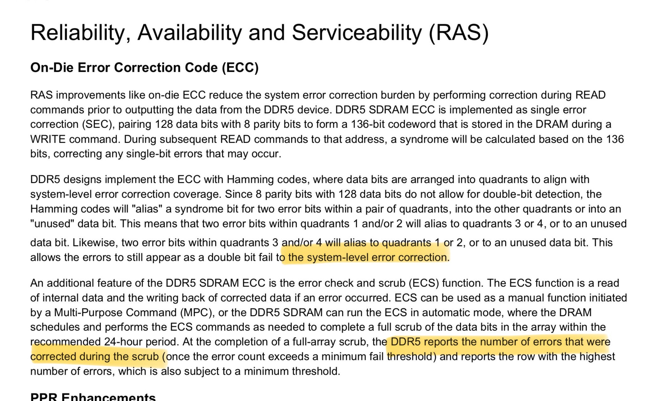
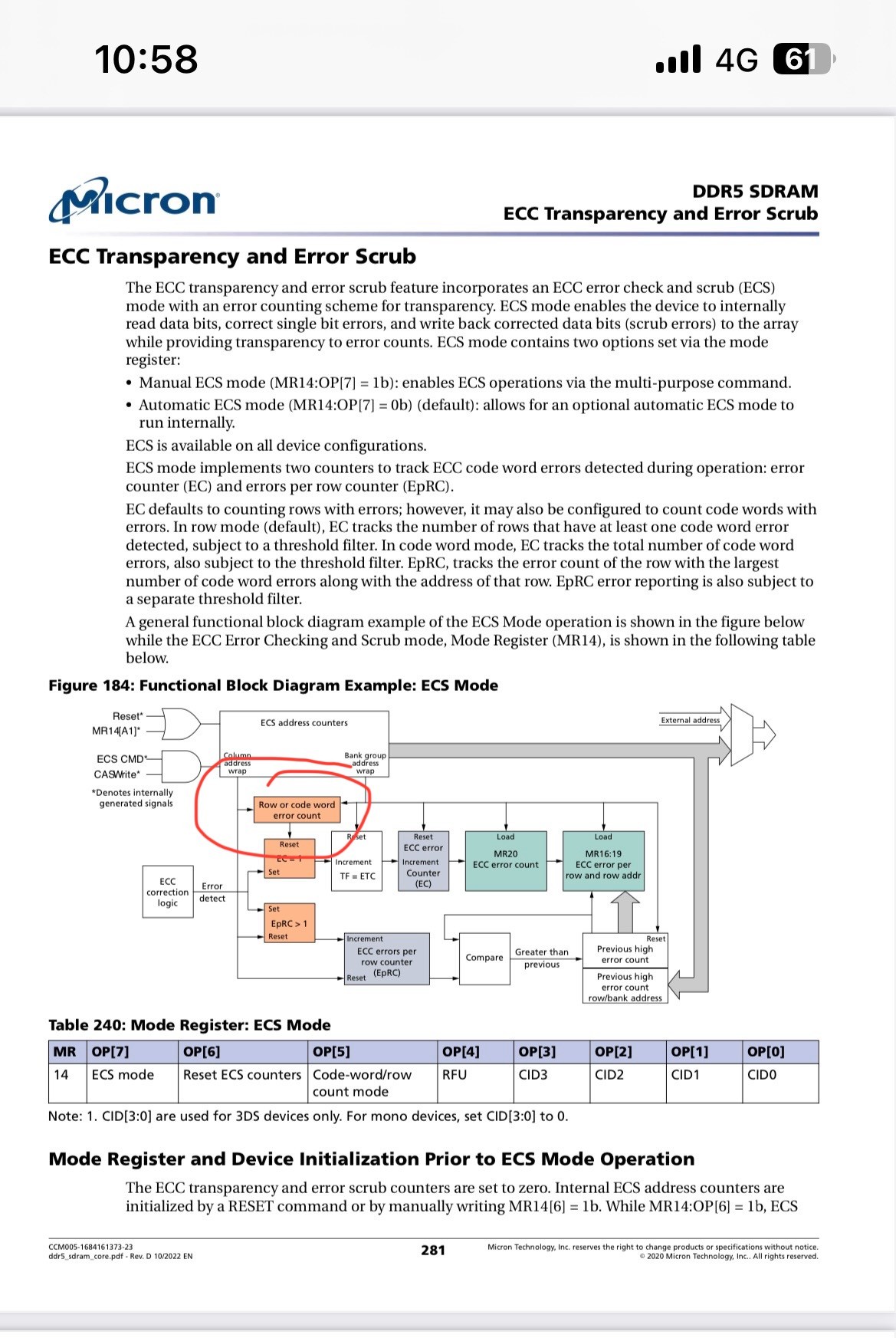
"here’s some excerpts from the standard DDR5 datasheet (the LPDDR5 datasheets are not publicly available) showing an internal Error Count “mode register” (that chipset can read) that I _think_ is incremented during regular error corrections, and a special command called “error scrub” which will do a full array read+correct+write+[report error count] upon request "
1701714866234.jpeg

1701714878707.jpeg


"also notice that even when announcing on-die ECC for DDR5, they still nod towards the need-for and existence-of system-ECC. Again, this is for DDR5. LP5 is similar, but LP5 specs are held much closer to the vest because of 1:1 relationships between memory suppliers and buyers. Unlike DDRx, which is often sold on open markets so all specs must be publicly available and fully standardized (or commodified)"
1701714916897.jpeg


"damnit. Too many screenshots and links to manage on a phone. Meant to attach this overview of the Error Scrub command, which finds, fixes and counts error on demand"
1701714947368.jpeg


Following this exchange I asked if he thought On-Die ECC in addition to Link ECC and reporting of errors was equivalent to traditional ECC. His response was:

" I’m not a system engineer (I’m a chip engineer), but in my opinion, yes. LP5 on-die ECC + Link-ECC (if enabled) is functionally equivalent to server style module-based ECC. _Perhaps_ even better in real world usage, data can be corrected in 2 places? (bc we know data is clean when it leaves the DRAM, therefore allowing more correctable errors than before in transit. That depends on the specific correction capabilities) But I don’t know actual system-level results to back that up"

"following up on Apples motivations… Discussing ECC implies that errors are possible. IMO, Apple would prefer to not even mention it. Because, truth be told, the _vast_ majority of people would never even consider that. “The chips make mistakes? How? Why?” So why even bring it up? The small amount of nerds who are actually aware of ECC systems may wring their hands, but so what? 99% of people buying Macs and iOS devices just take it as read that the chips “just work”"

So after all that, it does seem like it is possible that ECC is implemented. It all depends on whether Apple is using Link ECC. To my knowledge, without someone on the inside saying, we can’t know.

Looking at @leman patents, we can see some mentions of LPDDR5. The relevant parts I saw were:

"[0021] In some embodiments, the memory is an LPDDR5 memory that is configured to detect both link errors and on-chip errors. The memory controller may force a write link error correction code (ECC) error to maintain the poison status in this context."

"0054] The fifth generation of the Low-Power Double Data Rate (LPDDR) SDRAM technology was initially released in the first half of 2019. It succeeds its predecessor, LPDDR4/4X, and offers speeds of up to 6400 Mbps (1.5 times faster). Further, by implementing several power-saving advancements, LPDDR5 may provide a power reduction of up to 20% over previous generations. LPDDR5 may provide a link ECC scheme, a scalable clocking architecture, multiple frequencyset point (FSP’s), decision feedback equalization (DFE) to mitigate inter-symbol interference (ISI), write-X functionality, a flexible bank architecture, and inline on-chip ECC. LPDDR5 systems typically do not offer server-level reliability features such as single-device data correction (SDDC), memory mirroring and redundancy, demand scrubbing, patrol scrubbing, data poisoning, redundant links, clock and power monitoring/redundancy/failover, CE isolation, online sparing with automatic failover, double device data correction (DDDC), etc."

In conclusion, I don’t know.
 
Last edited:

mr_roboto

Site Champ
Posts
288
Reaction score
464
Thanks, I learned some new info! Much more reporting capability than I'd thought there was, though from what I skimmed through it looks like there's just counters to tell you that errors happened. Ideally you want to be able to at least partially log which addresses had errors - logging can be problematic to do perfectly but even a limited scope log can be very useful in tracing what went wrong.

Not too relevant on a consumer/prosumer platform, though. Apple's not building high-RAS servers.
 

theorist9

Site Champ
Posts
613
Reaction score
563
I think when people are complaining, they are complaining about link ECC? (Or they don’t understand the difference between them).

I’ve always felt link ECC was a dumb solution - just differential signal and you’re immune to injected noise. Twice the wires, but you also buy yourself immunity to a bunch of side channel attacks. Nobody listens to me.
Quoting from a discussion I had with @mr_roboto on another site (I want to give him credit for what he wrote), here are the key downsides of inline ECC (of which link ECC is one type) and sideband ECC:

"If it's an NVidia-like inline ECC system, then yes, you accept less capacity and bandwidth and worse latency. Sideband ECC (the kind found in conventional ECC DIMMs) doesn't hurt nominal memory capacity or bandwidth, but requires the DIMM to have 1.125x as much DRAM (as in, an 8GB ECC DIMM really has 9GB worth of DRAM chips on it) and costs more power - usually there's an entire extra DRAM chip, after all."

What would be the downsides of your approach, and if they are much less significant than those for the existing tech, why not submit a paper about it? [Alternately, can you patent it, or is there prior art and/or would it be considered too obvious?]
 
Last edited:

Cmaier

Site Master
Staff Member
Site Donor
Posts
5,329
Reaction score
8,520
Quoting from a discussion I had with @mr_roboto on another site (I want to give him credit for what he wrote), here are the key downsides of inline ECC (of which link ECC is one type) and sideband ECC:

"If it's an NVidia-like inline ECC system, then yes, you accept less capacity and bandwidth and worse latency. Sideband ECC (the kind found in conventional ECC DIMMs) doesn't hurt nominal memory capacity or bandwidth, but requires the DIMM to have 1.125x as much DRAM (as in, an 8GB ECC DIMM really has 9GB worth of DRAM chips on it) and costs more power - usually there's an entire extra DRAM chip, after all."

What would be the downsides of your approach, and if they are much less significant than those for the existing tech, why not submit a paper about it? [Alternately, can you patent it, or is there prior art and/or would it be considered too obvious?]

People already do what I’m talking about. Downside is it takes twice as many wires and drivers. But you can drive each wire half as hard and have the same noise margin.
 

theorist9

Site Champ
Posts
613
Reaction score
563
People already do what I’m talking about. Downside is it takes twice as many wires and drivers. But you can drive each wire half as hard and have the same noise margin.
Interesting--so no reduction in capacity or bandwidth, no increase in latency, and no need for added DRAM. I'm curious who does this, why more don't use this approach.

Is there a term of art for it, and is it supported as a form of ECC in any of the JEDEC standards? Are they able to call it ECC in their marketing materials?
 
Last edited:

mr_roboto

Site Champ
Posts
288
Reaction score
464
Interesting--so no reduction in capacity or bandwidth, no increase in latency, and no need for added DRAM. I'm curious who does this, why more don't use this approach.

Is there a term of art for it, and is it supported as a form of ECC in any of the JEDEC standards? Are they able to call it ECC in their marketing materials?
It's not a form of ECC at all. It's a different method of transmitting 0's and 1's which is much more noise immune than "single ended" signaling standards like those used in DRAM.

Single ended signalling sends 1 bit at a time through 1 wire by wiggling that wire between two voltage levels, one of which is mapped to logic-0 and the other to logic-1. When noise moves the voltage on this wire around, the receiver could falsely register a 1 as a 0 or a 0 as a 1.

Differential signaling sends 1 bit at a time through a pair of wires by requiring that transmitter send the nominal signal on one wire in the pair and an inverted copy of it on the other. So, when one wire is logic 0, the other is logic 1, and vice versa. The two wires only temporarily read the same voltage during transitions.

Why this helps: If you route the 2 wires of each pair right next to each other their whole length, keeping them a small distance apart, and make sure to keep the lengths equal, injected noise from outside interference sources should affect both wires in the pair equally. The receiver is built to interpret the wire pair based on the difference in voltage across the pair rather than caring about absolute levels. Since the voltage on wire 1 is X + noise and the voltage on wire 2 is Y + noise where X and Y are the logic 0 and logic 1 levels, when you subtract one from the other, the noise cancels itself out and you are left with X - Y (or Y - X).

There's many standards out there which use differential signalling - for example, PCIe. But DRAM has almost never used it, probably because it's really sensitive to cost. Differential needs 2x as many wires and chip pins for the same data path width. Beancounters are why nobody listened to Cliff on this one.

I say "almost" because somewhat recently, a consortium created a DRAM standard called "Hybrid Memory Cube". HMC DRAM devices were a stackup consisting of a logic/interface die on the bottom with several conventional DRAM die stacked on top of it. The logic die was a memory controller, and it interfaced to the rest of the system through high speed SERDES links - differential pairs. In HMC they tried to make up for the cost implications of differential by running relatively narrow SERDES links at much higher bit rates, up to 30 Gbps according to wikipedia's article.

What this made for in practice was very expensive and power-hungry memory, so it kinda fizzled out. HBM, a nominally similar concept, has had much more success by eschewing the SERDES differential interface.
 

theorist9

Site Champ
Posts
613
Reaction score
563
It's not a form of ECC at all. It's a different method of transmitting 0's and 1's which is much more noise immune than "single ended" signaling standards like those used in DRAM.

Single ended signalling sends 1 bit at a time through 1 wire by wiggling that wire between two voltage levels, one of which is mapped to logic-0 and the other to logic-1. When noise moves the voltage on this wire around, the receiver could falsely register a 1 as a 0 or a 0 as a 1.

Differential signaling sends 1 bit at a time through a pair of wires by requiring that transmitter send the nominal signal on one wire in the pair and an inverted copy of it on the other. So, when one wire is logic 0, the other is logic 1, and vice versa. The two wires only temporarily read the same voltage during transitions.

Why this helps: If you route the 2 wires of each pair right next to each other their whole length, keeping them a small distance apart, and make sure to keep the lengths equal, injected noise from outside interference sources should affect both wires in the pair equally. The receiver is built to interpret the wire pair based on the difference in voltage across the pair rather than caring about absolute levels. Since the voltage on wire 1 is X + noise and the voltage on wire 2 is Y + noise where X and Y are the logic 0 and logic 1 levels, when you subtract one from the other, the noise cancels itself out and you are left with X - Y (or Y - X).

There's many standards out there which use differential signalling - for example, PCIe. But DRAM has almost never used it, probably because it's really sensitive to cost. Differential needs 2x as many wires and chip pins for the same data path width. Beancounters are why nobody listened to Cliff on this one.

I say "almost" because somewhat recently, a consortium created a DRAM standard called "Hybrid Memory Cube". HMC DRAM devices were a stackup consisting of a logic/interface die on the bottom with several conventional DRAM die stacked on top of it. The logic die was a memory controller, and it interfaced to the rest of the system through high speed SERDES links - differential pairs. In HMC they tried to make up for the cost implications of differential by running relatively narrow SERDES links at much higher bit rates, up to 30 Gbps according to wikipedia's article.

What this made for in practice was very expensive and power-hungry memory, so it kinda fizzled out. HBM, a nominally similar concept, has had much more success by eschewing the SERDES differential interface.
Thanks for the detailed explanation -- I understand now. What you're describing is common mode rejection, and it operates on the same principle as my balanced audio interconnects, where two signals (analog, in this case) are transmitted along a twisted pair with opposite polarity, and the receiver only responds to the difference between the two.
But you can drive each wire half as hard and have the same noise margin.
Wouldn't the common mode rejection ratio typically be at least a few orders of magnitude, enabling you to achieve the same S/N with much less than half the voltage (or, alternately, give a much better noise margin at half voltage)?
 
Last edited:

Cmaier

Site Master
Staff Member
Site Donor
Posts
5,329
Reaction score
8,520
Thanks for the detailed explanation -- I understand now. What you're describing is common mode rejection, and it operates on the same principle as my balanced audio interconnects, where two signals (analog, in this case) are transmitted along a twisted pair with opposite polarity, and the receiver only responds to the difference between the two.

Wouldn't the common mode rejection ratio typically be at least a few orders of magnitude, enabling you to achieve the same S/N with much less than half the voltage (or, alternately, give a much better noise margin at half voltage)?
Yes, but in practice we halve the voltage because you still have situations where there can be single-ended noise. (With transistors it’s also tricky to reduce the voltage by more than that).
 

Cmaier

Site Master
Staff Member
Site Donor
Posts
5,329
Reaction score
8,520
On the differential thing, I should point out that my PhD project was the creation of a CPU that was entirely differential - very gate had differential outputs and every wire was actually a pair of wires routed next to each other their entire length.

That got me my job at Exponential Technology, where all of the data path portions of the processor used the same trick (I was the only person they hired who already knew how to do that).

Then my first case as a lawyer involved someone who claimed to own the idea of using differential signaling to suppress side channel attacks.
 

theorist9

Site Champ
Posts
613
Reaction score
563
On the differential thing, I should point out that my PhD project was the creation of a CPU that was entirely differential - very gate had differential outputs and every wire was actually a pair of wires routed next to each other their entire length.

That got me my job at Exponential Technology, where all of the data path portions of the processor used the same trick (I was the only person they hired who already knew how to do that).

Then my first case as a lawyer involved someone who claimed to own the idea of using differential signaling to suppress side channel attacks.
Feel free to use this as your CV cover if you ever apply to Apple. ;D
1701973237470.png
 
Top Bottom
1 2